Microscopy
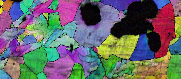
Our Microscopy Lab serves as a central hub for material characterization, offering in-depth insights into the microstructure of materials. Through state-of-the-art imaging and analysis techniques, we provide a detailed understanding of how microstructural features impact material performance and influence processing. This comprehensive analysis is essential for advancing research and industrial applications, allowing us to optimize materials for a wide range of cutting-edge technologies.
Optical microscopes
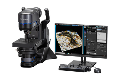
Several optical microscopes are available; the most upgraded version is Olympus DSX.
- Supplier & Model: Olympus / DSX1000 High-End model
- Testing methods: High res. and long working distance in one objective. Six observation methods: BF, DF, DIC, POL, OBQ right and left.
- 5 different objectives
- Motorized stage
- Tilting option for various imaging options
MIPAR software is available for image analysis
Scanning Electrong Microcope (FE-SEM)
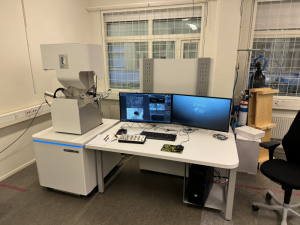
Hardware:
- TESCAN Mira 4th generation - Variable pressure
- Electron Backscatter Diffraction (EBSD); Hikari Plus (up to 1000 indexed points/sec)
- Energy Dispersive Spectrometry (EDS); Octane Elect (res. 127 eV for Mn)
- Wavelength Dispersive Spectroscopy (WDS); TEXS HP
- BSE detector motorized
- In-beam SE
- Plasma Cleaning system
- In-situ tensile/compression/heating stage, adaptable for in-situ EBSD applications (up to 5kN and 800°C) + extensometer; K&W
Software packages:
- Essence full package
- TEAM complete package + Particle analysis; EDAX
- TSL-OIM complete package
Dual beam electron microscope (FIB-SEM)
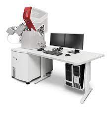
Hardware:
- TESCAN Lyra3 GMU - Variable pressure
- Electron Backscatter Diffraction (EBSD); Hikari Super (up to 1200 indexed points/sec)
- Energy Dispersive Spectrometry (EDS); Octane Plus (res. 127 eV for Mn)
- Wavelength Dispersive Spectroscopy (WDS); TEXS HP
- Scanning Transmission Electron Microscopy (STEM); BF,DF, HADF (res. down to 0.8 nm)
- Focused Ion Beam (FIB); COBRA (res. down to 2.5 nm)
- 4 Quadrant Backscatter Solid State Detector (4QBSE)
- Water-cooled BSE detector; for in-situ high temperature applications
- Nanomanipulator; Oxford OmniProbe200
- Beam Deceleration Mode; for low kV applications
- In-beam BSE; In-beam SE
- Low vacuum SE
- Plasma Cleaning system
- Field Cancellation System
- In-situ tensile/compression/heating stage, adaptable for in-situ EBSD applications (up to 5kN and 800°C) + extensometer; K&W
Software packages:
- Advanced tomography
- Automated TEM lamella preparation
- MeX Professional 3D surface imaging; Alicona
- 3D reconstruction; ORS Visual
- TEAM complete package + Particle analysis; EDAX; 2D and 3D
- TSL-OIM complete package
- CORAL for correlative microscopy
Atomic Force Microscope (AFM)
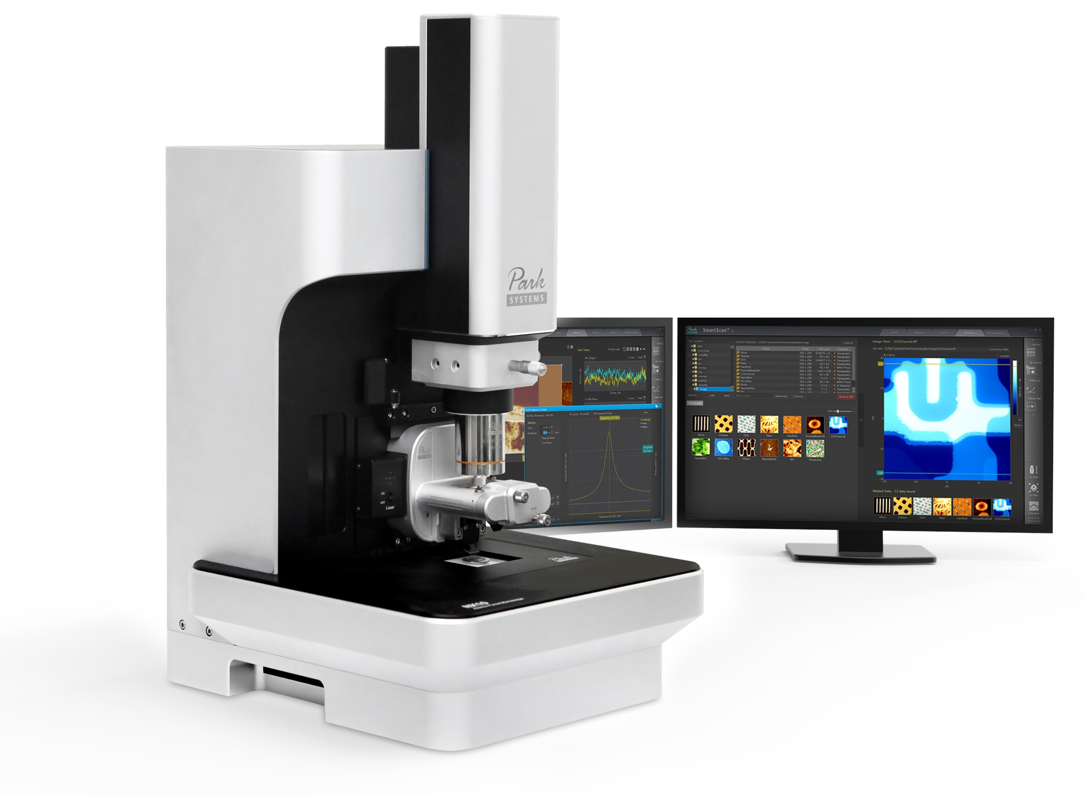
For topography and chemical potential measurements + nano-indentation
- Supplier & Model: Park / Nx40
- Type of Material for testing: metals, coatings; flat and max 20 mm height
- Testing methods: surface morphology (contact and non-contact), SKFM, nanoindentation, coupling with electrochemical cell for morphological studies under polarization in liquid
- Others: Max. 15 micron z range
Precision Etching-Coating System (PECS)
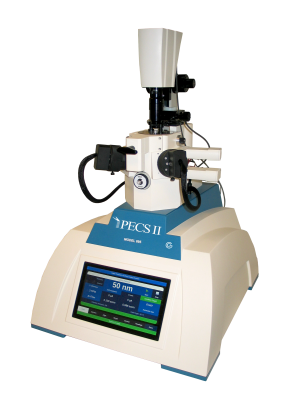
Fully automated argon ion polishing - Broad Ion Beam (BIB) milling
- Supplier & Model: Gatan / PECS II
- Type of Material for testing: all
- Testing methods: Precision milling of up to 1 cm in diameter, cross-secitoning of thin films and coatings, sputter coating for Carbon or Chromium
- Temperature range: RT down to -20C
- Sputter coating resolution of 0.1 nm
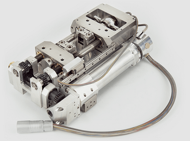
In-situ mechanical testing
Fully automated argon ion polishing - Broad Ion Beam (BIB) milling
- Supplier & Model: Kammrath & Weiss / 5kN module
- Type of Material for testing: all
- Testing methods: Tensile/Compression/Cyclic loading for up to 5 kN loading, up to 20 um/s withdrwal rate
- Temperature range: RT up to 800C
- Compatible for in-situ EBSD testing (tilted)
